Brushless DC (BLDC) Motor Design: A New Starting Point
Introduction
Brushless DC motor (BLDC) design is complicated. It doesn’t help that customers begin their electronics selection (old starting point) navigating through a maze of enormous; MOSFET, IGBT and Gate driver product portfolios.
onsemi is here to help, delivering a “new 1st order approximation starting point”, matching gate drive to switch (N-FET, or IGBT), much closer to the customer’s final decision, and leapfrogging the “old starting point” of seemingly endless product portfolio grazing. This includes 5 comprehensive tables incorporating motor voltages of; 12V, 24V, 48V, 60V, 120V, 200V, 300V, 400V and 650V, up to 6kW.

Figure 1
Brushless DC Motors (BLDC)
Brushless DC (BLDC) motors offer many advantages over brushed permanent magnet DC (PMDC) motors, specifically higher reliability, little to no maintenance, lower electrical and acoustic noise, better thermal performance, higher speed range, and higher power density. A typical BLDC motor uses permanent magnets on the rotor, and three armature windings (U, V, W) on the stator. A microcontroller (MCU) implements one of a variety of control and modulation schemes (trapezoidal, sinusoidal, FOC with SVM, DTC, etc.) to strategically energize the motor windings. This creates electromagnetic fields, causing an interactive force between the rotor magnets and the stator windings. When done properly, this interaction allows for precise control of the motor’s speed, torque, or power in the desired direction.
Figure 2 illustrates a typical block diagram of a 3-phase BLDC motor. The MCU executes the control and modulation scheme firmware, where it commands its PWM peripherals to output six coordinated duty cycles to three half-bridge gate drivers. These three drivers act as power steering for the six power MOSFETs in the output bridge, energizing the low-side (LS) and high-side (HS) U, V, and W MOSFETs. These are typically N-Channel MOSFETS rated for 1.5~2.0x the motor voltage, up to ~300V. Above 300V, N-Channel MOSFETs are typically replaced by IGBTs for their higher power performance.
The MCU can measure the current through each winding via the FAN4852, CMOS Op-Amp (9MHz typical BW), and optionally, can assess the rotor’s angular position with Hall Effect sensor feedback. Alternatively, a sensor-less architecture can be implemented with more processing overhead. The RSL10 BLE can be used for asset tracking, Firmware over the Air Updates (FOTA), feature selection/tuning, and telemetry data gathering.

Figure 2
BLDC Table #1: 12V & 24V (N-FETs) up to 1.1kW
Table 1 below lists a “new 1st order approximation starting point” for matching BLDC gate drive to N-Channel MOSFETs for 12V from 93W to 372W, and 24V from 186W to 1.1kW.

Table 1
BLDC Table #2: 48V & 60V (N-FETs) up to 1.5kW
Table 2 below lists a “new 1st order approximation starting point” for matching BLDC gate drive to N-Channel MOSFETs for 48V from 186W to 1.5kW, and 60V from 186W to 1.5kW.
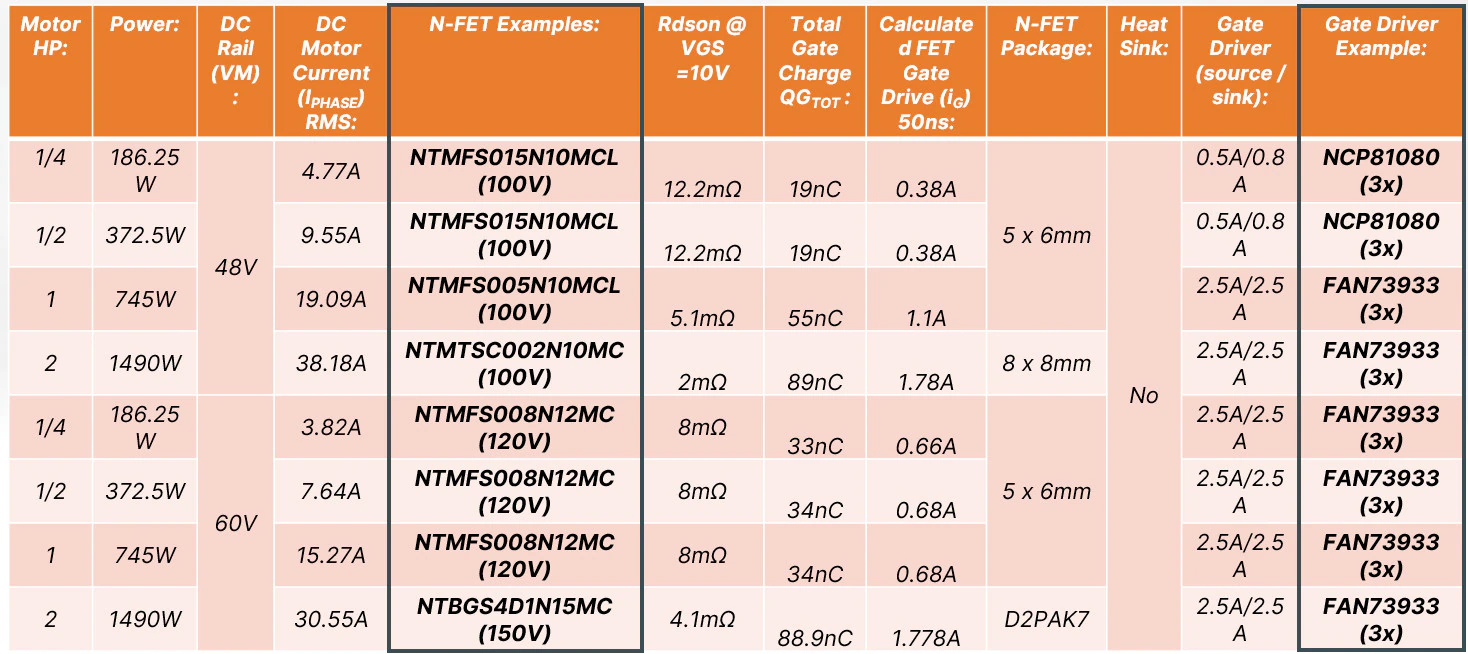
Table 2
BLDC Table #3: 48V & 60V (N-FETs) up to 3kW
Table 3 below lists a “new 1st order approximation starting point” for matching BLDC gate drive to N-Channel MOSFETs for 120V from 186W to 1.8kW, and 200V from 186W to 3kW.

Table 3
BLDC Table #4: 300V & 400V (IGBT’s) up to 6kW
Table 4 below lists a “new 1st order approximation starting point” for matching BLDC gate drive to IGBTs for 300V from 372W to 4.5kW, and 400V from 372W to 6kW.

Table 4
BLDC Table #5: 300V, 400V & 650V (IPMs) up to 6kW
Table 5 below lists a “new 1st order approximation starting point” for Integrated Power Modules (IPMs), where the gate drive and IGBTs are integrated into an easy to use module, for 300V from 372W to 4.5kW, 400V from 372W to 6kW, and 650V from 372W to 6kW.

Table 5
onsemi offers a great online tool for building BLDC with IPMs (Integrated Power Modules). The user enters 15 operating conditions and the tool produces multiple detailed Analysis Tables plus twelve graphs capturing critical thermal and power performance (Figure 3).

Figure 3
BLDC Tables #1 - #5
BLDC is complicated with hundreds of decisions to be made start to finish. For example, If you took 3 different customers; a, b and c (Figure 1), beginning at the same “starting point” (24V, 1 1/4hp motor), by the time all 3 customers navigated their respective decision trees, their final designs will be completely different. This is because each customer has their own threshold for cost, efficiency, power density, form factor, maintenance, lifetime etc. So, it is impossible to build gate drive to switch (MOSFET/IGBT) matching tables, and have it be correct for every customer. If we tried, we might be correct for one customer, and incorrect for another 999 customers. However, we can make some reasonable assumptions, based on intelligent engineering considerations, and produce a “1st order approximation” that lies somewhere between handing the customer Switch and gate drivers portfolios (old starting point: you are on your own), and the customer’s final decision.
1st Order Approximation Engineering Considerations
1) Cost: We strived to filter the lowest cost while meeting the following considerations.
2) Topologies: The Trapezoidal (a.k.a. 6-Step Control) Commutation was selected because it is relatively simple to control and yields high efficiency and high Peak Torque. Since only two power switches are on at any one time, each switch experiences a 33% “on time” duty cycle.
3) PWM Duty Cycle: PWM Frequency of 15 kHz. This is typical for most BLDC under 6kW.
4) Gate Driver: Junction Isolated Gate drivers. These tables do not include Galvanic Isolation.
5) Temperature: Ambient temp of 850C.
6) Gate Drive Calculation: The rated Gate drive is calculated by dividing the QG(TOT) (nC) by the ON/Off time (ns). We chose 50ns ON/Off for N-FETs, and 200ns for IGBTs.
7) N-FET Junction Temperature: (TJ) for surface mount packaging (no heat sink) is calculated by TJ = PDISS x RθJA + Ambient, leaving a minimum of 250C headroom below the maximum rated TJ.
- Where:
i. RθJA = Junction to Ambient thermal resistance
8) IGBT Junction Temperature: IGBT Junction Temperature (TJ) for through hole packaging with a heat sink is calculated by TJ = PDISS x (RθJC + RθCS + RθSA)+ Ambient, leaving a minimum of 500C headroom below the maximum rated TJ.
- Where:
i. RθJC = Junction to Case thermal resistance
ii. RθCS = Case to Heat Sink thermal resistance
iii. RθSA = Heat Sink to Ambient thermal resistance
9) N-FETs Power Dissipation: IPHASE2 (A) x RDSON (ohms).
10) IGBT Power Dissipation: Switching Loss + Conduction Loss + Diode Loss
- Where:
i. Switching Loss = Ets (J) x PWM Frequency (Hz)
ii. Conduction Loss = IPHASE (A) x VCE(SAT) (V)
iii. Diode Loss = (switching loss + conduction loss) x 0.25
11) Switch Voltage Rating: N-FET V(BR)DSS and IGBT VCES = 2-3x Motor Voltage
12) Switch Current Rating: N-FET ID and IGBT IC = 3 x IPHASE.
13) Motor Phase Current: IPHASE = 1.23 x POUT / VBUS
- Where:
i. IPHASE = Motor Phase Current, Amps
ii. POUT = Electrical Power Output of Inverter to Motor
iii. PF = Motor Power Factor, 0.0 – 1.0, 1.0 is ideal (we assume 0.85)
iv. VBUS = Motor Bus Voltage, VDC, or 24V
v. MI = Modulation Index, 0.0 – 1.0, typical is 0.9 (we assume 0.9)